Pull up your bootloader
In this study you will see that you don't always have to use expensive equipment to uncover these pins, sometimes all you need is a scope, a decent camera and knowing what you're looking for.
Vous souhaitez améliorer vos compétences ? Découvrez nos sessions de formation ! En savoir plus
Introduction
SoC designers include the capability to customize the hardware behavior according to pin state at system boot, when the /RESET signal is de-asserted, just after power up. These pins states are controlled through a set of pull-up and pull-down resistors, altering the default configuration. For instance, the core clock frequency, some multiplexed pins configuration, or bootloader source can be adjusted before the CPU runs any code. Changing the bootloader source is what we want to try to do in this study.
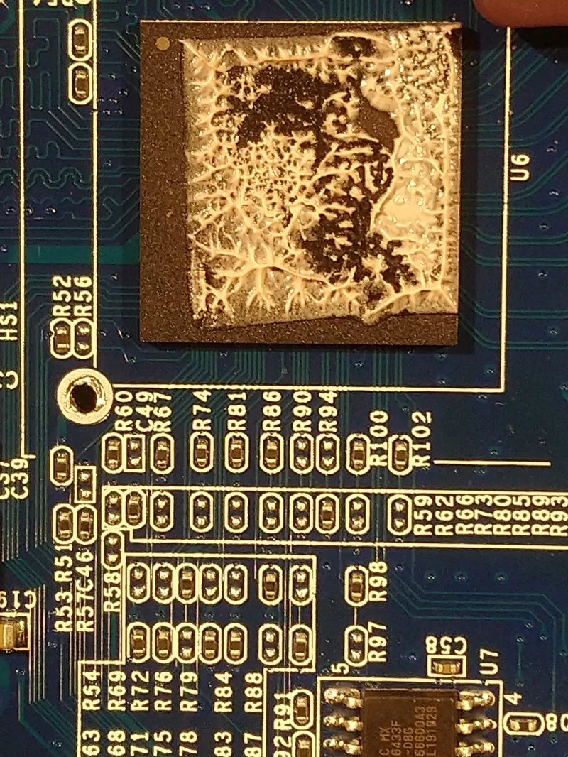
The SoC is often packaged on a substrate mounted on balls, known as BGA style package. This package family prevents the observation of tracks between balls and other components on the board, as this substrate is obviously not transparent. The picture below shows the studied SoC package side view, focusing on balls located on its border.
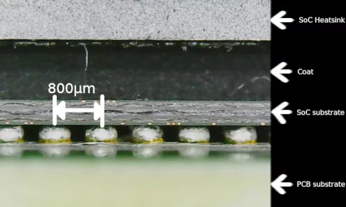
There are 10 rows of balls like that one before reaching the center of the package.
A workaround consists in de-soldering the SoC substrate (destructive), or to use high-end photographic technique (X-rays1).
We will see that by knowing a couple of initial data, we can still partially deduce the path between some SoC's hidden balls and the rest of the board.
In order to figure out the exact or possible resistor role in the configuration word, we will rely on the following three input vectors :
- the configuration word value
- the SoC pin map
- the observed paths of resistors
Once resistor roles are identified they can be populated or unpopulated, which consequently impact the resulting configuration word.
The remaining tricky stage is to guess the invisible tracks between pins under the SoC's substrate and the rest of the board elements.
Case study
Some ARM-based SoCs belonging to the "Kirkwood" family, from MARVEL company, can read the bootloader code from several sources such as a NAND or NOR Flash, a serial line, a PCIe or SATA connected device. The boot mode typically comes from its configuration word.
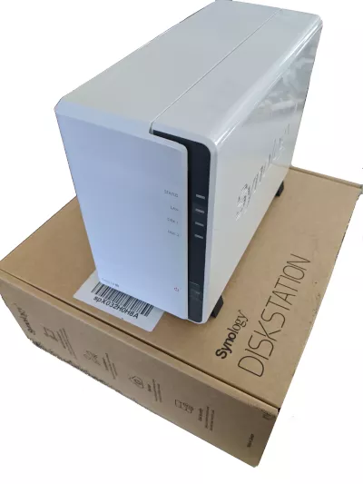
The POC has been exercised on a SOHO NAS system containing all initial requirements: the DS218j NAS from Synology company. It contains indeed the well-documented Kirkwood 88F6280 SoC, boots over a FLASH memory, and supports SATA bus.
The goal of the POC is to boot the SoC from the disk, bypassing genuine FLASH code execution, by identifying and modifying the right pull-up and pull-down resistors defining the reset configuration word.
Configuration word
The 88F6280 chip has no fewer than six pins to control the bootloader source, which give the choice -theoretically- between 64 bootloader sources. Hopefully, not every combination is a valid boot mode.
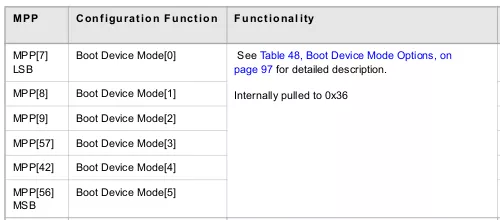
Strangely enough the default boot source 0x36 seems invalid, or at least not documented officially.
Valid boot values, as detailed page 97 of the datasheet, are summed up for you in the following table.
	Boot device  Bootloader
	   value      source
	[0x00-0x05]:  NOR
	[0x08-0x1f]:  NAND
	[0x26-0x27]:  SPI NAND
	[0x28]:       UART
	[0x2a]:       SATA LANE#0
	[0x2b]:       SATA LANE#1
	[0x2c-0x2d]:  PCIe
	[0x30-0x31]:  SDIO
	[0x32]:       SPI NOR /CS#0 24 address bits
	[0x33]:       SPI NOR /CS#0 32 address bits
	[0x34]:       SPI NOR /CS#1 24 address bits
	[0x35]:       SPI NOR /CS#1 32 address bits
The SoC booting on a 8MB SPI Flash (MX25L6433F), we can guess that the current boot device mode is set to 0x32 "SPI NOR /CS#0 24 address bits". This hexadecimal value is translated into 110010 in binary format. Once mapped on MPP[x] pins, it means that:
|
MPP pin |
Expected value |
|---|---|
|
|
0 (LSB) |
|
|
1 |
|
|
0 |
|
|
0 |
|
|
1 |
|
|
1 (MSB) |
That's the very easy part. The value of the 17 other pins involved in the configuration word is harder to figure out. Let's cheat a little bit and read the registers reflecting the MPP[x] pin status once the SoC is fully functional. Don't blame me, the goal of the study is to guess the hardware tracks, not the configuration word.
Once booted under Linux, DS218j system allows SSH connection. Using this channel to connect with root privileges, the SAR ("Sample At Reset") register content, located at physical address 0xf1018600, can be extracted. This register reflects the MPP[x] value as latched on /RESET signal de-assertion. Its value is a gold mine as it shows up the exact pull-up/pull-down state at SoC power on. Exactly what we are looking for.
Believe me or not, its value is 0xcb20a324 on the DS218j board.
All things considered, the full relationship between the SAR bits, as read in the SAR register, the MPP pins and their respective values are depicted in the following table.
|
SAR bit# |
MPP pin# |
Value |
Nibble |
|---|---|---|---|
|
0 |
28 |
0 |
0x-------4 |
|
1 |
10 |
0 |
0x-------4 |
|
2 |
23 |
1 |
0x-------4 |
|
3 |
11 |
0 |
0x-------4 |
|
4 |
7 |
0 |
0x------2- |
|
5 |
8 |
1 |
0x------2- |
|
6 |
9 |
0 |
0x------2- |
|
7 |
57 |
0 |
0x------2- |
|
8 |
42 |
1 |
0x-----3-- |
|
9 |
56 |
1 |
0x-----3-- |
|
10 |
33 |
0 |
0x-----3-- |
|
11 |
30 |
0 |
0x-----3-- |
|
12 |
31 |
0 |
0x----a--- |
|
13 |
34 |
1 |
0x----a--- |
|
14 |
35 |
0 |
0x----a--- |
|
15 |
29 |
1 |
0x----a--- |
|
16 |
4 |
0 |
0x---0---- |
|
17 |
32 |
0 |
0x---0---- |
|
18 |
22 |
0 |
0x---0---- |
|
19 |
N/A |
0 |
0x---0---- |
|
20 |
1 |
0 |
0x--2----- |
|
21 |
51 |
1 |
0x--2----- |
|
22 |
N/A |
0 |
0x--2----- |
|
23 |
N/A |
0 |
0x--2----- |
|
24 |
N/A |
1 |
0x-b------ |
|
25 |
N/A |
1 |
0x-b------ |
|
26 |
N/A |
0 |
0x-b------ |
|
27 |
36 |
1 |
0x-b------ |
|
28 |
44 |
0 |
0xc------- |
|
29 |
47 |
0 |
0xc------- |
|
30 |
N/A |
1 |
0xc------- |
|
31 |
N/A |
1 |
0xc------- |
That is the "truth" table, it will be the key to identify the resistors connected to the SoC pin.
For instance, the bit#0 of the SAR register, reflecting the state of the MPP[28] pin at reset de-assertion, is a logical 0, which means that we expect a pull-down on that pin.
Now that we have the truth table, which give us valuable hints about pull-up/pull-down resistor expected presence and the accurate pin location, let's dig into the hardware part.
SoC pin map
Having a sight to the PCB, we can guess, on the front face, the Kirkwood SoC under its flat heat sink, the RAM package at its upper left corner, a SPI FLASH on the bottom right corner, and a couple of differential pairs in the upper right.
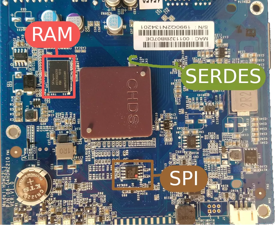
The tracks related to SERDES2 are well recognizable due to the paired pattern, with some little zigzag counteracting the track length difference from end to end within a pair.
The back face contains a few integrated chips and many discrete components.
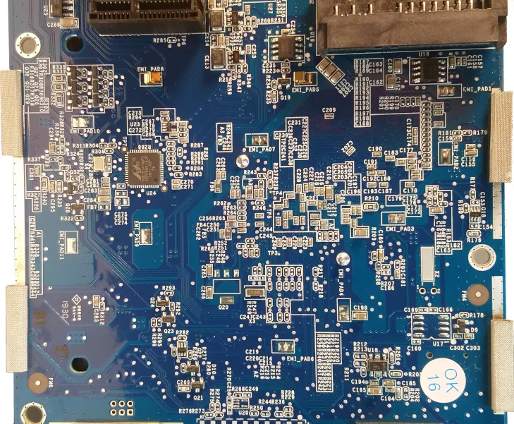
One can roughly project the heat sink placeholder thanks to its two big soldered anchors, and deduce approximate SoC substrate footprint.
The tracks reverse engineering seems overwhelming on this back side. We will see that it is actually the easiest part.
From a macroscopic point of view, one can notice that the RAM package and SERDES tracks in the front side match their respective location relative to the SoC pinout, as supplied by the SoC manufacturer. Don't panic with the number of pins (388 exactly), near half of them are dedicated to power supply, gathered mostly in the center of the chip.
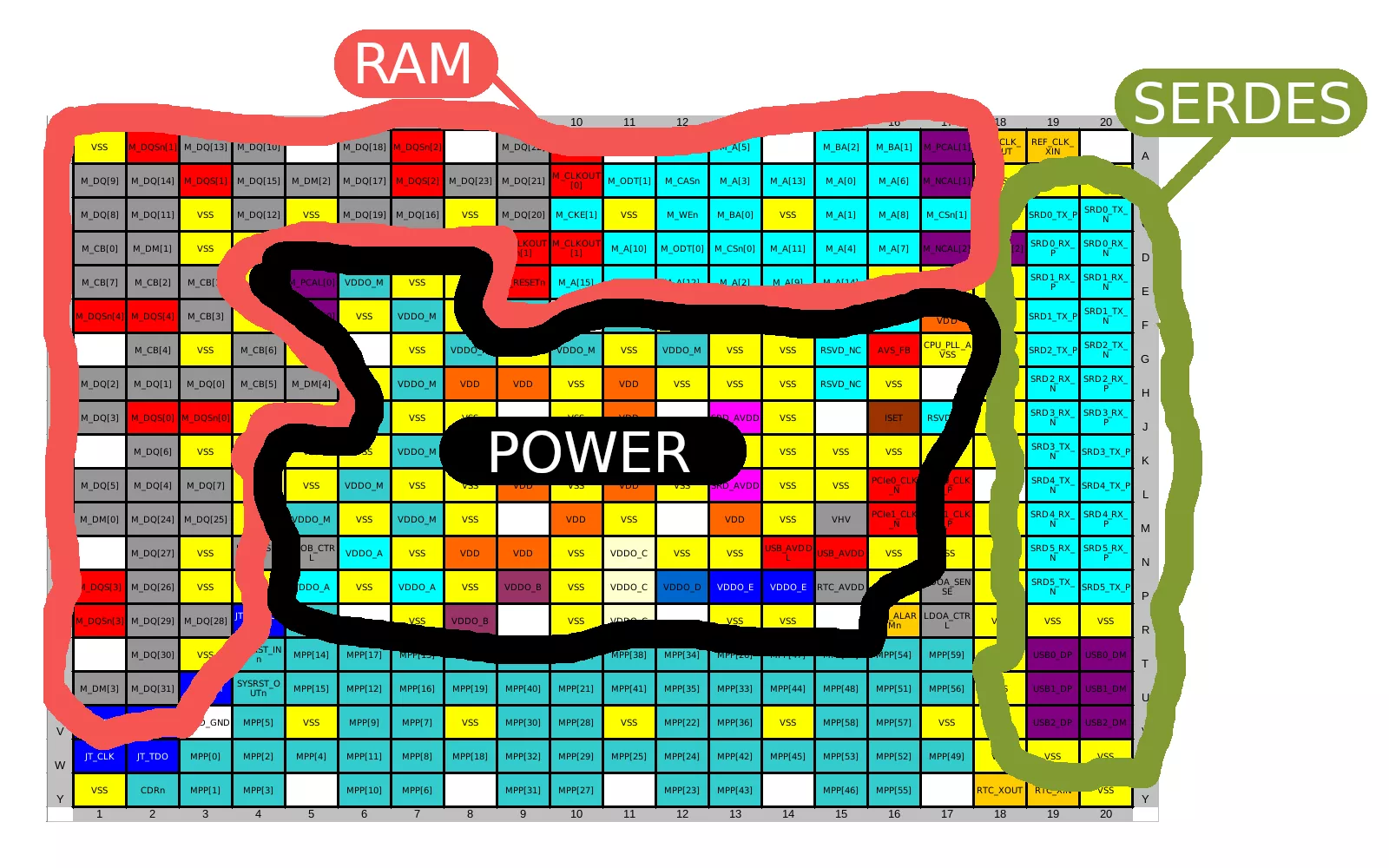
Apart from SERDES, RAM, power supply (VSS and VDDx), resets (SYSRSTx), miscellaneous clocks and JTAG pins, most remaining connections are related to so-called MPP[x] pins. Theses MPP[x] pins are simply multiplexed inside the SoC, dedicated to various classical functions as GPIO, I2C bus, SPI bus, UART, PCIe etc. The actual function of each pin is software configurable.
Let's go deeper in the identification of these pins -under which a strange group of resistors are soldered- by simply highlighting the MPP[x] pins involved in the configuration word.
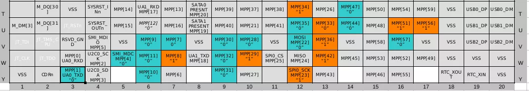
This picture is declined from the previous manufacturer genuine pin map, coloring MPP[x] pin boxes implied in the configuration word, graying all other pin boxes. Furthermore, the expected logical values have been reported from the truth table we built in the previous chapter. For instance, the MPP[1] pin, located at Y3, which function may be UART TX3, is expected to be pulled down according to the truth table in order to be sampled "0" at /RESET de-assertion.
The MPP[23] and MPP[22] are also directly mapped to the SPI function, as we do know a SPI Flash memory is connected to the SoC.
One can wonder why we highlight all MPP[x] pins involved in the configuration word while we only need, at most, to identify the six bits related to the boot mode. In fact, the more featured pins we have, the more chance to figure out the connection under the BGA we have.
Let's get more accurate, and map the known pin features on the physical SoC map. The manufacturer, in the hardware datasheet, reveals the exact ball positions relative to the substrate boundary from the bottom view.
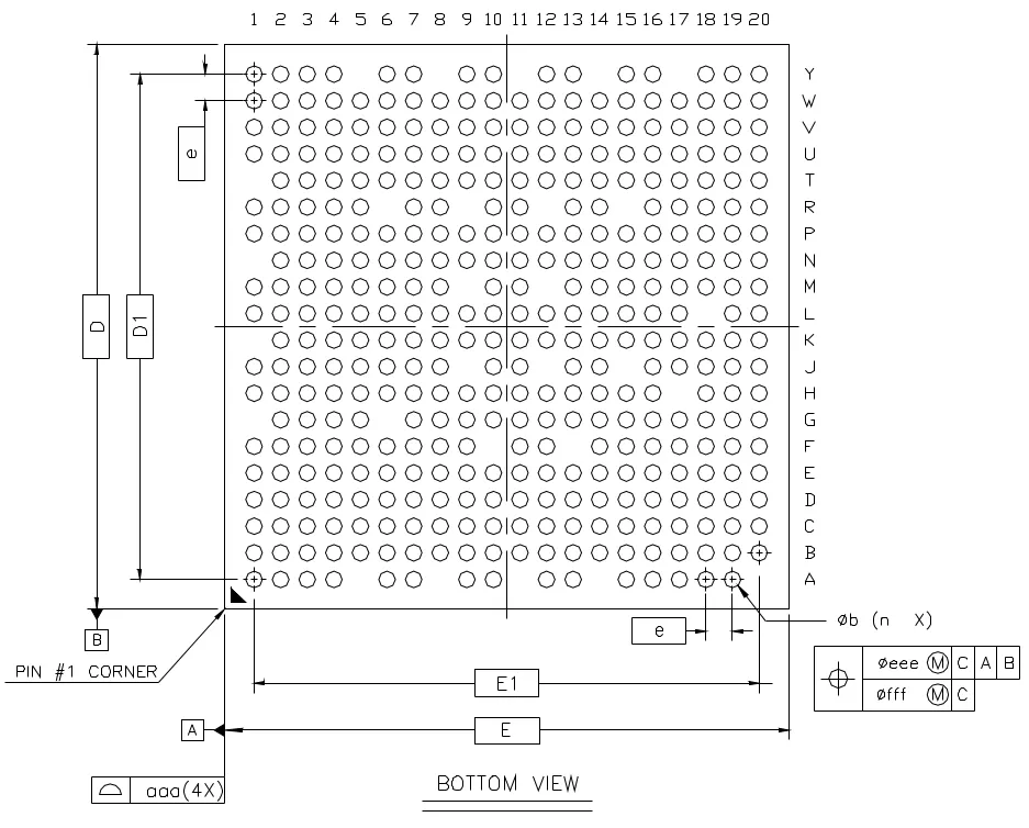
Let's play with GIMP and annotate our key pins. The picture below is the "bottom" part of the SoC pins physical implementation zoom in. Using totally arbitrary colors, power supply balls have been colored in black and JTAG pins in dark blue. The MPP[x] pins involved in the configuration word which the subject of our interest here, are colored either orange or magenta if they are expected as a logical '1' or '0' at /RESET de-assertion. Let's forget all other -kept white- pins.

Now let's map the expected pin values over the real SoC picture, greatly enhancing reality.
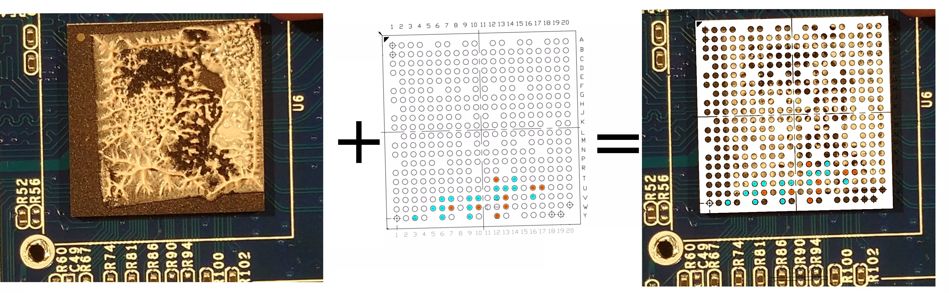
Playing with GIMP layers, after reflecting and aligning front and back side images using via holes in the PCB as guides, we can synthesize the equivalent on the back side. The following picture reveals the location of the balls soldered on the front side, seen from the back side.
MPP tracks
A bunch of resistors between the SoC and the SPI Flash caught our attention, so closely located near the MPP[x] pin area.
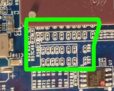
A couple of resistors also appear in the back side of the PCB in the same area (not shown here for the moment). Definitely interesting. Let's carefully remove the SoC heat sink as it hides valuable tracks between the hot MPP[x] pins area and the resistors bunch.
By powering up the board, we can analyze the signal of each resistor bound with an oscilloscope. It quickly appears that most of them are either linked to the ground or to the 3.3V power rails. Same thing on the back side.
Note: when the oscilloscope equipment is not available, one can use a multimeter setup on 'continuity test' mode while the board is powered off. Electric continuity can be observed between resistors bound and a reference ground point or a 3.3V reference point. However, different power rails may be present on the board (mostly 3.3V for I/O but also 1.8V for (R)GMII GEthernet bus for instance). In this case, the tester may lie while checking continuity between a pin driven at 1.8V and the ground reference point: it may tell you it finds a perfect electric continuity.
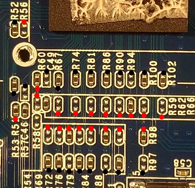
Red points highlight the 3.3V power pads while black points are tied to the ground lane.
By converting a 3.3V into a logical "1" value and ground into a logical "0" value, the tracks entering the SoC package look like the following:
In this picture, tracks associated to a pull-down or pull-up resistors have been highlighted in green, while tracks to the SPI FLASH are in violet. At last, brown tracks appear on the left (UART RX), in the bottom middle (SATA present signals?), and on the right (to an undetermined destination, but neither pulled up nor down).
For clarity, pull-up and pull-down state, translated into logical value, have been clearly reported in the border of the coat, before invisibility area, in red. An "X" letter appears on a weird track that supports resistor pads for a pull-up and a pull-down without being actually populated.
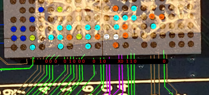
Running the same exercise in the back side reveals the following enhanced tracks, terminated by its pad and the measured logical value.
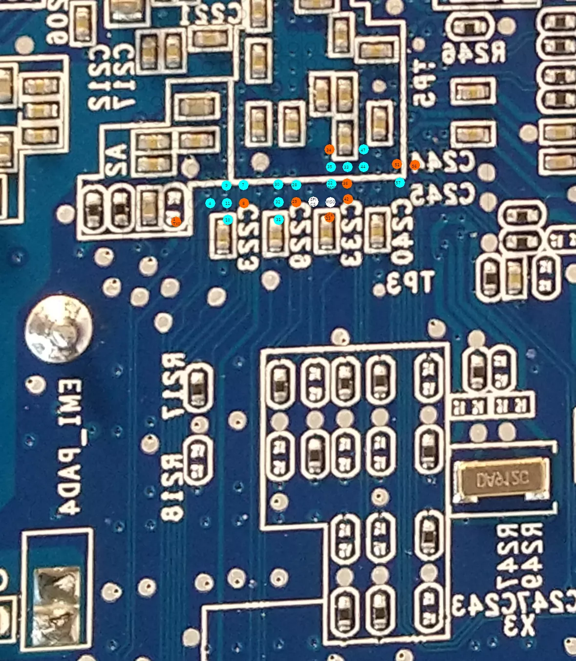
Now let's merge this picture, focusing on the tracks termination under the SoC balls, with the SoC balls locations, as we extrapolated them on the back side.
Pretty sure, the MPP[56], at the full right, expected as a logical "1", is soldered to the right track. Idem for the next MPP[51] pin. With the same confidence, the MPP[34] ball is soldered to the nearest track tied to a logical "1".
Note that the confidence greatly depends on the accuracy with which we can apply the ball physical location to the PCB image. In these low resolution PCB photos, it is far from being perfect.
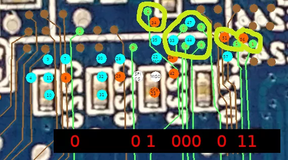
The group composed of MPP[33], MPP[47] and MPP[44] -tied to logical "0"- cannot be deterministically associated to their tracks. Hopefully, our initial configuration word doesn't involve these pins.
The full left track is too far from any MPP[x] pin implied in the configuration word: even if pulled down, the track must hold a functionality at runtime (not only a configuration bit) undiscovered so far.
The 2nd left track, tied to logical "0", may be connected to the MPP[28].
So far, 4 resistors have been associated to the MPP[x] pin with good confidence, and a group of 3 resistors remains associated to a group of 4 tracks pulled down. Unfortunately, none of which we are focusing on to modify the bootmode (MPP[7,8,9,57,52,57]).
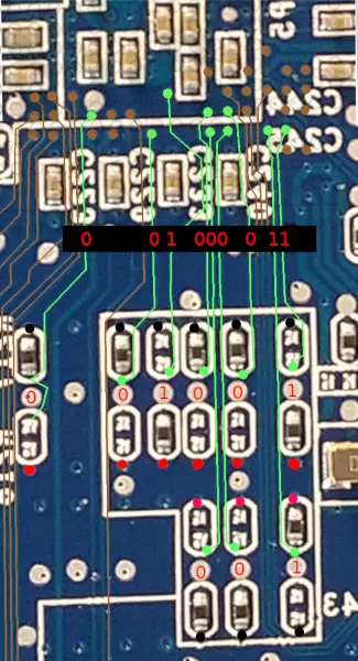
Back to the front side, it remains at most 16 MPP[x] pin tracks to recover. Let's run the same forecast exercise.
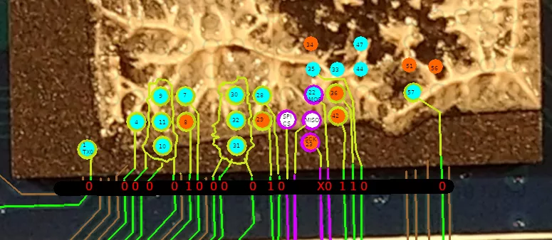
From left to right, the MPP[1] ball (also used as UART TX) is linked to the first track without doubt, the MPP[4] is very probably linked to the second green track. Then a group of 3 balls are somewhat linked to the next 3 tracks, implying MPP[9], which is involved in our bootmode configuration. Damn.
The fifth and sixth green tracks are clearly linked to MPP[8] and MPP[7], implied in the bootmode configuration.
Next again a group of three tracks tied to ground are linked to 3 balls MPP[30],MPP[32] and MPP[31], in an undetermined order. Next MPP[29] and MPP[28] are surely linked to the following tracks, and the next four violet tracks are fully reverse engineered by linking them to the SPI package.
The next two tracks tied to "1" are very probably linked to MPP[42] and MPP[36].
The two last tracks tied to "0" are very probably linked to MPP[35] and MPP[57].
Remaining balls involved in the configuration word are linked to tracks on the back side, already reversed.
Bootmode resistors
By combining all guessed tracks, we can reconstruct -at least partially- the relationship between the 6bits bootmode word and resistors references:
|
Pin# |
Bootmode bit# |
Pull-up/down resistor |
SPI bootmode value
|
SATA#0 bootmode value
|
SATA#1 bootmode value
|
|
|
0 |
(R73) / R74 |
0 |
0 |
1 |
|
|
1 |
? |
1 |
1 |
1 |
|
|
2 |
? |
0 |
0 |
0 |
|
|
3 |
(R101) / R102 |
0 |
1 |
1 |
|
|
4 |
R93 / (R94) |
1 |
0 |
0 |
|
|
5 |
? |
1 |
1 |
1 |
Amazing, we got every resistor locations needed to change the bootmode from the 0x32 value to 0x2a or 0x2b !
Warm up the solderer, remove the R102 and R93 resistors, move them to the opposite resistors and that's it: the SoC should boot over the SATA disk instead of the SPI Flash.
Unfortunately, it fails.
Plug-in any old-school spinning HDD disk into any of both SATA connectors available, nothing happens.
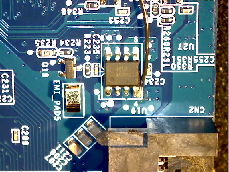
The first reason is due to the energy-saving mechanism implemented in this NAS: power is NOT propagated to the SATA connector automatically when the board is powered up. Further investigation by reverse-engineering tracks around the MOSFET chip located near both SATA connectors could workaround the missing power. Now HDD disks are spinning on board power up by forcing the gate pin of the MOSFET 4953 responsible for SATA power supply.
But no more signs of live yet.
Reverse engineering SERDES tracks reveals that the SATA connector #1 is NOT connected to the very first SERDES pair lines, nor the SATA connector #2 to the second SERDES pair lines.
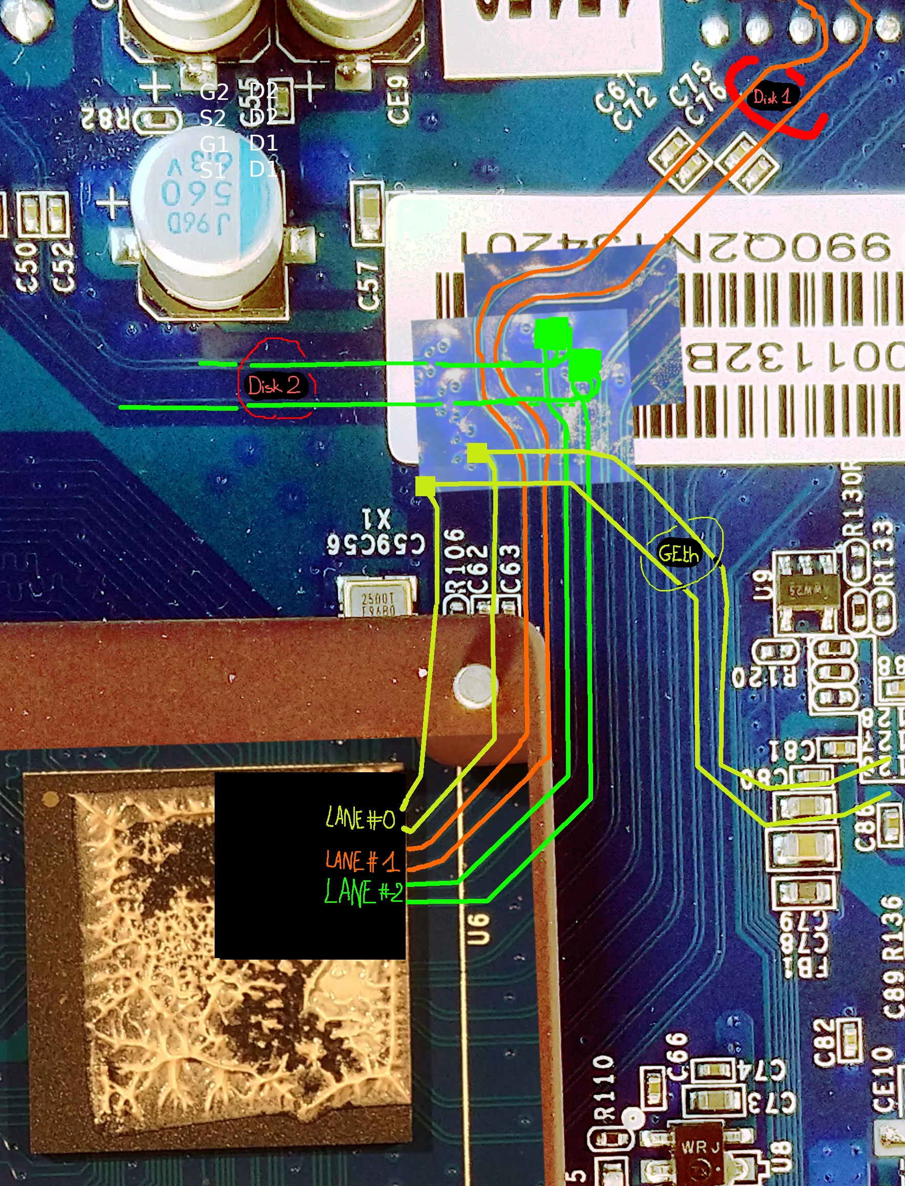
Instead of the trivial layout, the disk#1 is connected to the SERDES LANE#1 and disk#2 to the LANE#2, while the GEthernet occupied the first SERDES lane (notice the cross lanes just under the barcode sticker!).
From bootrom point of view, the SATA#0 device must be connected to the SERDES LANE#0. Thus, the currently modified resistors layout would boot on a SATA device that would be connected... in the place of the GEthernet controller. No way.
Hopefully, the bootmode also supports booting on SATA#1 device, on SERDES LANE#1, where the disk#1 is connected. Finally, we must modify a last resistor R74 to force the bootmode word to 0x2b (SATA#1) instead of 0x2a (SATA#0).
After copying the SPI content into the disk and tweaking a CRC4, the serial console shows the following traces at power-up.
BootROM - 1.73
Booting from AHCI
Probing HBA- 0 port 0  SATA device found


## THIS BOOTLOADER HAS BEEN MODIFIED ##
AVS selection from EFUSE disabled (Skip reading EFUSE values)
Overriding default AVS value to: 0x23
Detected Device ID 6820
High speed PHY - Version: 2.0

Init Synology board board SerDes lanes topology details:
 | Lane # | Speed|    Type     |
 ------------------------------|
 |   0    |  0   |  SGMII0     |
 |   1    |  6   |  SATA0      |
 |   2    |  6   |  SATA1      |
 |   4    |  5   |  USB3 HOST0 |
 |   5    |  5   |  USB3 HOST1 |
 -------------------------------
High speed PHY - Ended Successfully
DDR3 Training Sequence - Ver TIP-1.46.0
DDR3 Training Sequence - Switching XBAR Window to FastPath Window
DDR3 Training Sequence - Ended Successfully
Mission completed.
Conclusion
With common equipment such as a consumer-grade smartphone camera and a low-cost USB magnifying glass, one can accurately follow PCB tracks from end to end. While BGA-based package prevents full reverse engineering to chip pins, considering the signal context held by tracks greatly helps figuring out the tracks last millimeters, as we showed it here.
The technique limit is the number of layers used to compound the PCB. Fortunately, the system used in this POC hides only the power tracks between each visible layer. Modern and very high density PCB are compounded of more than four layers. In these cases more expensive techniques, either in terms of reverse engineering equipment or time spent, must be used.
- 1. The hardware version, not IDA.
- 2. SERDES are common blocks converting data between serial data and parallel interfaces in each direction.
- 3. As it will be verified later
- 4. The original string "General initialization - Version: 1.0.0" has been replaced by "## THIS BOOTLOADER HAS BEEN MODIFIED ##".