Car hijacking swapping a single bit
Looking to improve your skills? Discover our trainings sessions! Learn more.
Security Access
For integrity and security obvious reasons, the critical interactions with an ECU must be granted to authorized persons only. A dedicated service is available in the UDS standard for this purpose: the famous Security Access request. Based on challenge/response authentication, the underlying protocol is up to the constructor. In the study case, the challenge is issued from a random number appended to various key identifiers of the car, sent to the user (named Tester in the UDS world) as a seed. The Tester then sends back a response based on this seed ciphered with a secret key. When the answer doesn't match the value computed within the ECU, the Tester remains in a limited spectrum of allowed commands. On contrary, when the ECU validates the answer, mainly all available interactions are possible. Profit.
Bruteforcing the secret key is especially time consuming, or just painful when the constructor implements anti-bruteforce techniques. Anyway, the constructor specific authentication algorithm must also be published somehow.
On the other side, the authentication bypass may be easier when the UDS server delegates the authentication response check to an ancillary chip which it communicates with in clear text over the wires. In the study case, the main chip running the UDS server asks an ancillary chip to validate the Tester's response over a SPI link.
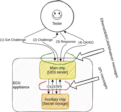
The final message (4) between the ancillary chip and the main chip is a singular point of failure during authentication validation: if it can be forced to the "OK" value, the main chip is tricked and believes the Tester is legitimate.
Serial link protocol MiTM
The software on the master chip is considered as a white box (software is available) but not the ancillary chip. The only thing we know about the ancillary chip is its location on the ECU board, its manufacturer reference, its documentation (publicly available on the Internet). The authentication algorithm and the secret key are unknown.
This chip package leaves all pins fully accessible to play with electronic probes (contrary to BGA family ones).
On the other side, this ancillary chip has multiple pins with two, three or more functions, meaning that a pin can be used for ADC, CAN, PWM, SPI, whatever according to an internal configuration: the pins dedicated to the SPI link are dynamically defined at boot-up, not hard-wired. Let's discover them.
Locating pins
Knowing that the SPI link is -by definition- based on a clock signal, all pins have been blindly probed until finding a signal that beats eight times in a row, periodically.

Bingo, that is a signal with the eight edges corresponding to the eight bits to transmit, beating at a frequency of 4.8 MHz. With the help of the MCU documentation, poking around this clock pin reveals which pins are carrying the MOSI and MISO signals.
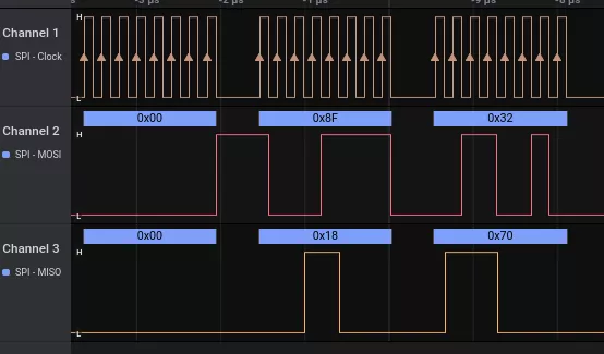
The extract above shows the MOSI (master to slave) line sending three bytes while the MISO (slave to master) sends synchronously its own payload[1]. Zooming out this signals sample shows that the software protocol encapsulates data within 128-byte frames. This will be confirmed by the analysis of the protocol stack on the master chip. Zooming out yet more shows that the 128-byte SPI frames are spaced, in the higher rate, by a 300us rest period. That seems to be the highest bandwidth at which the master is able to output bytes. Believe me or not, the observed maximum throughput is roughly 1.7Mb/s which is rather slow compared to nowadays communication bandwidth.
The SPI pins are definitely located. Great. Let's flip one or two bits on the slave authentication response and trick the master.
Flipping one or two bits, easy no?
TL;DR: it depends for whom.
Technically, we are trying to setup a MiTM (Man in The Middle) attack on the SPI link, especially on the upstream link, from the slave to master (MISO signal). From a first approach, the MiTM appliance is composed of a slave SPI receiver coupled to a slave SPI emitter and a little bit of computation in between.
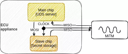
The MiTM appliance de-serializes the MISO signal issued from the slave chip, analyses stream byte by byte, and pushes back the same or patched byte to its upstream link according to its internal state, paced by the master's clock. Yes, but... practically, do you know which simple chip contains a processor and a slave SPI interface? When a processor is coupled to a SPI interface, it generally wants to be the master, not the slave. Actually, it exists some cheap on-the-shelf appliances, typically Arduino boards or STM32-based systems that can do the job. Functionally, it integrates a processor and a slave SPI interface. Let's go and code.
Wait... remember the 520ns between each byte in the first SPI clock samples diagram. Does a cheap processor run fast enough to handle an interrupt triggered by the SPI receive interface, process a couple of bytes and load the SPI transmit register before the first bit of the next byte starts to be emitted?
As a rule of thumb, a 1.3GHz ARM-based SoC spends around 100ns handling an external interrupt in the ideal execution conditions: no OS, single core dedicated to this interrupt, warmed up caches, shortest assembly-coded interrupt handling path. Any data or code cache miss will explode this figure. Needless to say that I/O memory access between the processor and a peripheral controller does not take the same memory-optimized bus. On the contrary, the I/O bus (to the SPI interface for instance) may even be much slower than the memory bus.
In these conditions, it seems unreliable to read the incoming byte, process it, write the next one within the rough 500ns timing window with a cheap SoC. Any late transmission would break the protocol and be fatal.
One will argue that SoC can easily achieve 1Gb/s (and much more) throughput, where this case is limited to a maximum of -ridiculous- 1.7Mb/s in sustained stage. But these high throughput are reach bypassing processor execution path, relying on an external engine dedicated to bunch of memory copies, also called DMA (Direct Memory Access). This solution is not affordable in the study as -at least- one byte must be patched on-the-fly within one of the 128-byte SPI frames, implying a minimum of processing.
End of the game? No, a solution resides in the four following letters: FPGA.
Hardware design
An FPGA (Field-Programmable Gate Array) is a highly configurable integrated circuit containing many elementary logic blocks. Using combinatorial logic clocked at a couple of nanoseconds, this solution appears reasonable to achieve the bit flip in this time-constrained context.
On the other side, being a software developer, this hardware solution is rather unsettling, requiring to choose:
- a programming language, between so-called VHDL and Verilog,
- an FPGA founder, say Xilinx and Intel (ex-Altera), implying its specific design tools (named Vivado and Quartus),
- a final FPGA development board.
The programming language has been chosen without scientific argument: a quick search of tutorials for a noob on the Web showed more implementation examples wrote in VHDL than in Verilog. Notice that this result is fundamentally influenced by the search keywords and may easily produce an inverted result. Be that as it may, the selected programming language for the project is VHDL.
Concerning the founder, the choice mainly comes from experiences. Indeed a previous study implying the Vivado tool suite left a nasty feeling related to the overall slowness of the tool suite. Furthermore, an experienced fellow claimed to me that the Quartus GUI was much more user-friendly than its competitor. Fine, all essential elements are available to start at least the FPGA design based on VHDL in the Quartus suite. Let's see the FPGA board latter and start coding, at last.
In the first approach, the MiTM appliance must 'just' inject a bit or a couple of bits, overwriting the original slave response, at the right time. Schematically, it can be represented as a simple commutator on the SPI link, activated under the control of a brain continuously spying the incoming bit stream to detect the overwriting point.

For sure, this basic electronic component, known as a multiplexer, even a trivial two-entries one way multiplexer, will be quickly implemented in VHDL, even for a software developer. Furthermore, the compare function, seeking a 16-bit pattern ('xy' in the diagram above) should also be quickly implemented. At last, a slave SPI component, implemented in VHDL, de-serializing and re-serializing bytes, is also available at least on a GitHub project[2]. Just mix them all together and it will do the job.
Alas, this initial approach is definitely too high level.
First of all, studying the proprietary protocol used between both entities quickly revealed that each 128-byte SPI frame contains a 24-bit CRC (Cyclic Redundancy Check) trailer. That is rather a good idea in the industrial world in order to detect one or several spurious bit splitting, but quite annoying for a MiTM appliance quick design. Modifying a single bit within the SPI payload implies recomputing the CRC over the entire frame, otherwise the master chip drops the frame systematically. Implementing a CRC24 (or CRC16 or whatever CRC) in VHDL is not obvious for a completely un-experimented VHDL designer. Multitude CRC24 exist, depending on polynomial terms chosen[3]. Once again, Google is your friend: a web site[4] offers VHDL (and Verilog) implementation of all CRC of the world. Just specify the input width, the output format and your polynomial terms, and profit of the JavaScript-produced VHDL source code. It appeared -latter in this project- that the CRC computation is especially easy to implement in hardware, in fact.
In order to shorten the story (and avoid the constructor's information disclosure), the inner dual CRC16 computation is not developed here, nor the occult padding byte at the end of some SPI frames, neither the inner protocol embedded in the underlying protocol with its own header and payload spread over several SPI frames.
In a nutshell, the VHDL design development took much more time than expected, due to initially unidentified issues from an un-experimented hardware designer, but partially compensated by a rich documentation related to VHDL development[5].
Design simulation
As described in all manuals for beginners, the design has been validated entity by entity, thanks to the vital VHDL simulator available with the Quartus suite. First by de-serializing and re-serializing a single byte, then grabbing an entire 128-byte SPI frame, then computing and checking CRC over a single frame, and so on, until patching the right byte at the right place within a stream of hundreds of SPI frames. By the way, a wonderful feature used in the testbench is the ability to read data (used as test vectors) from a file formatted in CSV. The initial sampling tool (Saleae) recorded around two minutes of communication between the master and the slave, producing more than 2K SPI frames, in CSV format, ready to inject in the testbench, greatly simplifying tests over real vectors.
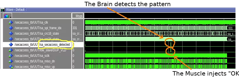
The final design detects the security access response among the 331 of SPI frames of the testbench (captured from the real slave activity), patches it on the fly, fixing all CRCs. Theoretically at least. Internally clocked at 100MHz, the design easily processes each incoming bit clocked at 4.8MHz. Thanks Quartus.
Play it
Unfortunately, the limited time allocated to this study is incompatible with current cheap FPGA board delivery latency. Electronic part market is under pressure and this attack could not be played for real within the blogpost timeframe.
Nevertheless, with partial knowledge of the communication protocol between two parts of this particular car ECU, the main diagnostic security access protection could have been bypassed with a cheap hardware part programmed with standard tools.
This first design and logic simulation open new perspectives for the next challenges implying hard real-time MiTM attack !
- [1]. Extra signals considerations as chip select, data sampling at falling or rising front edge, most or least signification bit first are deliberately omitted for clarity.
- [2]. https://github.com/jakubcabal/spi-fpga/blob/master/rtl/spi_slave.vhd
- [3]. https://users.ece.cmu.edu/~koopman/crc/crc24.html
- [4]. https://www.easics.com/crctool/
- [5]. https://vhdlguide.readthedocs.io/en/latest/