Code Check(mate) in SMM
Looking to improve your skills? Discover our trainings sessions! Learn more.
Some time ago I started reversing an AMI firmware from a quite up-to-date computer (2017/2018). While I was reversing a System Management Mode (SMM) driver, I noticed an interesting code change... during initialization, the SMM driver search for a SMM configuration table with a GUID named EFI_SMM_RUNTIME_SERVICES_TABLE_GUID1.
The result, if any, was then used as a classical EFI_RUNTIME_SERVICES table for providing some basic services to the driver including access to UEFI variables. The GUID name is pretty straight forward but I checked anyway and, as expected, the EFI_SMM_RUNTIME_SERVICES_TABLE is a runtime services table implemented in SMM.
At that point I was appreciative of this code change: it must have killed a lot of bugs. SMM, an Intel mode which is initialized during boot by the firmware, is partially in charge of protecting the firmware and also has full access to the memory (including kernel and hypervisor), which makes for a quite interesting target for an attacker.
This mode, sometimes called "ring -2", has its own reserved memory space, called SMRAM, which is protected from access by any code not in SMM. Before the previous patch, if code in SMM called the normal EFI_RUNTIME_SERVICES (which are not located in SMRAM), it would trigger one of the most basic and common vulnerabilities: a callout of SMRAM which is basically similar to a kernel executing code under userland control.
The reason why this is such a common vulnerability is that UEFI DXE2 drivers can provide protocols to each other, those protocols are simply tables (usually containing function pointers) identified by a GUID. If a SMM driver tries to use a protocol from a "normal" driver, it will probably end-up calling a function and trigger a callout of SMRAM. So I started looking for use of normal protocols by SMM drivers, and at that point I got suspicious: after reversing various drivers I did not found a single use of "normal" protocols.
This got me thinking, checking all those protocols would be pretty time consuming for firmware developers. That's when it hit me: they must have activated SMM_CODE_CHK_EN .
SMM_CODE_CHK_EN
SMM_CODE_CHK_EN is a single bit in the MSR MSR_SMM_FEATURE_CONTROL (Enhanced SMM Feature Control, 0x4E0), the official description of this bit being the following:
This control bit is available only if
MSR_SMM_MCA_CAP[58] == 1. When set to '0' (default) none of the logical processors are prevented from executing SMM code outside the ranges defined by the SMRR. When set to '1' any logical processor in the package that attempts to execute SMM code not within the ranges defined by the SMRR will assert an unrecoverable MCE.
While it is not available on all processors, it is not a really recent feature and most computers have it for a while. The description is pretty clear in itself, the SMRR are two MSR (IA32_SMRR_PHYSBASE and IA32_SMRR_PHYSMASK per core) indicating the range of the physical RAM provided for SMM, the SMRAM, and forbidding any access to it if the logical processor is not in SMM. If SMM_CODE_CHK_EN is enabled, it forbids code executed in SMM to be outside of the SMRAM. The activation of this flag is often compared to be an equivalent of SMEP3 for SMM.
According to the Intel documentation, the entire MSR_SMM_FEATURE_CONTROL is "Accessible only while in SMM". Regarding this, the first thing I did to confirm that SMM_CODE_CHK_EN was indeed enabled was to look in the firmware for a driver writing this MSR. At one point later in time, I tried to read it from outside of SMRAM and was surprised to see that I retrieved its value. I was later able to confirm this behavior on other computers, and it seems that this is not a unique problem but an "error" in the Intel documentation.
Another more important feature is the fact that the MSR_SMM_FEATURE_CONTROL has a Lock bit which, once set, forbids changes to the register. I checked if the Intel documentation did not make another "error" but I was not able to change the value of this MSR from SMM or from outside once it was locked. This means that once the feature is enabled and locked we can't just remove it, and we have to bypass it.
At that point I was sure that I finally got my hand on a firmware with SMM_CODE_CHK_EN activated. I remembered reading the blogpost from @d_olex where he bypassed this feature by patching code and data in SMM. In his post, he used the rewrite primitive from his vulnerabilities for modifying code and data before making a memcpy of his shellcode in SMRAM and executing it.
I was interested in trying to bypass it by myself and in particular I was interested in the case where we don't have an arbitrary write in SMRAM but just a simple call to an arbitrary address. As I said at the beginning of this blogpost, using a protocol which was created in the "normal" world will use a table (in normal world) containing pointers, which will then be called and trigger a crash because of SMM_CODE_CHK_EN . If we modify those pointers, we will be able to execute code in SMM, however this code must be located in SMRAM. What I wanted was a reliable way to exploit this kind of vulnerability while being the most firmware agnostic.
Bypass
Mapping code
Code from SMM is initialized by the firmware and, like the firmware's code, the usual memory protections we are used to are not enabled: code and data are readable, writable and executable, there is usually no canary and we are far away from any kind of ASLR. This has a tendency to make exploitation pretty simple as any kind of write will allow you to change code. However, two computers will often have at least a few different drivers and some hardware changes, which as a consequence would change the memory layout. This latest point can make difficult to write an exploit portable between two different vulnerable firmware. And now we also have the equivalent of SMEP.
The first step to address these issues will be to avoid relying on a leak or hard-coded addresses inside of SMRAM when mapping shellcode. When a System Management Interrupt (SMI) is triggered, the processor will switch in SMM, but before doing that it will first store some information about the state before the SMI, which is necessary for being able to restore the context when the processor switch out of SMM (which is done by using the rsm instruction). Those data are stored in a region called the SMRAM State Save Area: the exact position and content of this region depends on the architecture (32bits or 64bits) and we will consider in the rest of this blogpost that we are in 64bits.
The idea should however work fine for a 32bits processor. The SMRAM State Save Area is located between SMBASE+0xFC00 and SMBASE+0xFFFF, SMBASE being an address set when initializing SMM, which defines two things: the address at which the first code is executed when entering SMM (SMBASE+0x8000) and the address of the SMRAM State Save Area. Both of those must be located inside the SMRAM protected memory and, to complicate things a little, there is one SMBASE for each logical processor, which is needed since if two processors get into SMM at the same time, we don't want them to rewrite each other SMRAM State Save Area.
What's interesting about this SMRAM State Save Area is that it contains lots of information under an attacker's control when a SMI (and even better a SWSMI) is triggered. In particular it saves all of the normal registers in it with the following form:
typedef struct _ssa_normal_reg {
    UINT64 r15; // start at SMBASE + 0xFF1C
    UINT64 r14; // 0xFF24
    UINT64 r13; // 0xFF2C
    UINT64 r12; // 0xFF34
    UINT64 r11; // 0xFF3C
    UINT64 r10; // 0xFF44
    UINT64 r9;  // 0xFF4C
    UINT64 r8;  // 0xFF54
    UINT64 rax; // 0xFF5C
    UINT64 rcx; // 0xFF64
    UINT64 rdx; // 0xFF6C
    UINT64 rbx; // 0xFF74
    UINT64 rsp; // 0xFF7C
    UINT64 rbp; // 0xFF84
    UINT64 rsi; // 0xFF8C
    UINT64 rdi; // 0xFF94
} ssa_normal_reg_t;
At that point the idea is pretty simple: map your shellcode into the registers and jump with your exploit at the place where they are mapped. If we can control all those registers, we can put a shellcode of up to 0x80 bytes, which should be more than enough for doing everything that we want.
In reality, it is possible that a few of those registers are used by the SWSMI handler4 for getting the data from the OS: when triggering a vulnerability in a SWSMI handler those registers will often be constraint for being able to trigger the vulnerability. However, from what I have seen, the r8 to r15 registers are rarely used for this (the most common seems to be rbx, rcx and rdx or rsi and rdi depending of the firmware), which leaves us with 0x40 controlled (this may have to be adapted depending of the situation).
In order to test this idea, I created a really simple shellcode:
mov     edx, addr_wr
mov     dword ptr [rdx], 0xAABBCCDD
I set addr_wr to an address outside of SMRAM, initialize the memory at zero and trigger the SWSMI which will allow me to jump on the shellcode. At that point I hit a wall: it did not work. My first thought was that I could not execute my registers and I started to get a lot of theory on what could be the issue.
The answer was really much simpler. I used chipsec5 from an UEFI Shell for triggering my SWSMI with the registers set as a shellcode, and a little bug in chipsec implementation on UEFI made this fail: the code gathering the arguments from python for calling the swsmi function considers the arguments as 32bits instead of 64bits6. Once this was fixed the previous shellcode worked fine and we are now sure that the idea works.
Once I got execution in SMM, there are usually two really simple shellcodes I like to use, the first one being the simple idea of moving the value of the SMBASE. The SMBASE can be changed by rewriting its value in the SMRAM State Save Area (offset 0xFEF8) and returning from SMM. The next SMI will use the modified SMBASE, we just have to make sure that SMBASE+0x8000 is not in the range of the SMRR and write our code at that place for getting code execution in SMM. Sadly this shellcode will not work anymore: the SMM_CODE_CHK_EN will prevent our code from being executed because it is not in the SMRR range.
The second one is even more simpler: I just disable the SMRR, which allows to read and write in the SMRAM from outside of SMM, making the following steps of exploitation obvious. I was actually curious of how the SMM_CODE_CHK_EN feature would react to disabling the SMRR and decided to try it out. The shellcode for disabling the SMRR is really simple, it is enough to write 0 in the MSR IA32_SMRR_PHYSMASK (0x1F3), which contains the bit "Valid" indicating the SMRR are enabled:
mov ecx, 0x1F3
xor edx, edx
xor eax, eax
wrmsr
Sadly, this does not work and disabling the MSR seems to activate SMM_CODE_CHK_EN. Another idea I could have tried was to combine both previous shellcodes for moving at the same time the SMRR and the SMBASE address. In theory, this should work because the code executed at the next entry in SMM will still be in the range of the SMRR. Instead of doing that, however, I decided that with 0x40 bytes of shellcode I could do whatever I wanted, including simply read or write the content of the SMRAM with a simple memcpy shellcode:
mov ecx, size
mov esi, src
mov edi, dst
rep movsb
At that point, I can just use this shellcode for getting a SMRAM dump and then rewrite what I want, including the code of a SWSMI handler, and take control of SMRAM. This technique works well, we can put a shellcode in our registers and jump on them for code execution. However in order to be able to jump on the location where our registers are stored we need to know the address of SMBASE. This is a point I have left on the side until now, so let's try and answer the question: "How to get SMBASE?".
Getting SMBASE
The SMBASE is configured at boot by the UEFI firmware and can obviously change between firmware, this is a classic problem of exploitation on SMM and will probably be one of the first things you want to get once you have found a vulnerability. If you are able to make runtime analysis (meaning having hardware access and no problem if the computer crash) there are two known ways to retrieve SMBASE which are really efficient.
The first one is to inject a SMM driver in the firmware: during boot, the driver will be loaded and will give you access to the SMRAM, allowing code execution7. Once you are in SMM you can just get the SMBASE using a protocol or, even better, by reading the MSR IA32_SMBASE (at 0x9E)8. This technique is probably the most efficient one if you have physical access to the computer, but there is one drawback: if the firmware (correctly) implements Intel BootGuard9, the integrity of the boot components will be verified and the computer should shutdown when it detects a change in the signature.
The second technique is to simply try to bruteforce the SMBASE. The first and really simple shellcode I presented before is a perfect test for bruteforcing the SMBASE if you have an arbitrary call. All firmware I have encountered align the SMBASE on 4KB (0x1000) and it is enough to bruteforce between SMRR_BASE - 0x8000 and SMRR_TOP - 0x10000, which usually is not that big of a range. The biggest drawback of this method is that it will probably crash your computer at least once or twice before succeeding. Overall, it usually takes me around 1 hour to bruteforce the SMBASE.
Those two techniques are fine if you have full access and control of the computer, but I was interested in the case of a remote attack. I did not have any great idea on how to get the SMBASE so I started looking at one particular firmware. The first thing I checked was if there was an easy leak of the SMBASE through a standard structure available in memory: I dumped all the available memory from outside of SMM and looked for anything which could contain the SMBASE, but got no result. I then started to look in the firmware for where was the SMBASE setup and found the driver PiSmmCpuDxeSMM.efi, which is an open-source driver available in EDK2, but it seems to have been modified a bit.
Because of the necessity of having one SMBASE per CPU and the way the offset in it works, the different SMBASE are usually differentiated by a step between them, this is called the TileSize in the open-source code. The calculation of the TileSize in the firmware with the driver was made by the following code:
mov     r13, 0 ; init at the beginning of the function
mov     r14, 1
; [...]
calcTileSize:
mov     rax, rcx ; this is the start of the TileSize calculation with rcx as input
mov     r8d, 0FFFh
neg     rax
and     rax, r8
lea     rdx, [rax+rcx+0FFFh]
cmp     edx, r13d
jnz     GetPowerOfTwo32

mov     eax, r13d ; this is an error case and will never be reached
jmp     end
GetPowerOfTwo32:
; this is inline but the same as the open-source code from edk2, until the end label
mov     ecx, 1Fh
jmp     loop_condition
start_loop:
sub     rcx, r14
add     edx, edx
loop_condition:
cmp     edx, r13d
jg      start_loop
mov     eax, r14d
shl     eax, cl
end:
lea     ebp, [rax+rax]
This is a really simple code with just the function GetPowerOfTwo32 which will find the first higher number which is a power of two. The only input of this code is the rcx register which is initialized previously in the function at one of 3 possible value: 0x118, 0x11D and 0x134. The resulting TileSize is stored in the ebp register. It is obvious from this code that whatever the input, the resulting TileSize will always be 0x2000. Meaning that if we know one of the SMBASE we will be able to determine the others by just adding or subtracting 0x2000 bytes to their address.
That's good to know but we still need to determine the position of one of the SMBASE. Following that code, some more calculations are made to compute the total memory required to reserve before allocating it with EFI_SMM_SYSTEM_TABLE.SmmAllocatePages, the open-source code uses AllocateAlignedCodePages which is simply a wrapper on top of SmmAllocatePages.
By default (with Type = AllocateAnyPages equivalent to AllocateMaxAddress) the EDK2 implementation of SmmAllocatePages will first try to get a page from a freelist and if not available it will try to get the maximum address available. The thing is SMM drivers are also mapped in memory using this function, and there are really few cases where you will want to free something which has been allocated with SmmAllocatePages . This means that the address of the memory reserved for the SMRAM is probably just below PiSmmCpuDxeSMM.efi driver's address. We know that the higher SMBASE will be at 0x10000 bytes below the address of the driver and that every SMBASE structures are separated by 0x2000 bytes from each other.
Thing is, we don't have the address of the PiSmmCpuDxeSMM driver. However, while I was looking at the open-source code for the PiSmmCpuDxeSMM driver, I noticed an interesting line of code:
//
// Install the SMM Configuration Protocol onto a new handle on the handle database.
// The entire SMM Configuration Protocol is allocated from SMRAM, so only a pointer
// to an SMRAM address will be present in the handle database
//
Status = SystemTable->BootServices->InstallMultipleProtocolInterfaces (
    &gSmmCpuPrivate->SmmCpuHandle,
    &gEfiSmmConfigurationProtocolGuid, &gSmmCpuPrivate->SmmConfiguration,
    NULL
    );
This code installs a protocol for the "normal" world with a pointer on gSmmCpuPrivate->SmmConfiguration. The structure gSmmCpuPrivate is located in this driver, meaning that this actually provides the normal world with a pointer inside the PiSmmCpuDxeSMM driver. I checked the firmware driver and the code is indeed present. As I am working from an UEFI Shell, I just wrote a quick UEFI Application for requesting this protocol and getting the address, from an OS it would be necessary to parse the memory and look for the GUID, then find where the pointer is. Once I had the address of the protocol, I could just make the difference with its offset in the binary and get the address of the driver. So at this point I know the address of the PiSmmCpuDxeSMM driver and I know that the memory look like this (with n = number_of_cpu - 1):
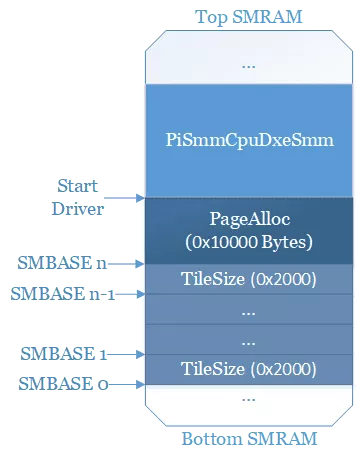
Getting the address of the first SMBASE has become a really simple calculation: SMBASE0 = addr_driver - 0x10000 - 0x2000 * (number_of_cpu - 1) . I checked it and it worked just fine.
Getting the SMBASE statically was finally a pretty simple thing, but all firmware do not use the same calculation and do not setup their SMBASE the same way, so this is not a really generic method. This is still better than having to craft a ROP chain for getting code execution in SMRAM; and basically everything we used came from the open-source implementation of EDK2 which still makes it, at least a little, portable between different firmware.
Conclusion
In summary, if we consider we have found a vulnerability allowing to call an arbitrary address in SMM, the final steps for the exploitation are:
- Get SMBASE:
LocateProtocolforgEfiSmmConfigurationProtocolGuidto have a leak of an address inPiSmmCpuDxeSmm.- Using the leak, compute the base address of
PiSmmCpuDxeSmm. - Determine the
TileSize(0x2000in our case). - Determine the address of the first SMBASE with the calculation:
addr_driver - 0x10000 - TileSize * (number_of_cpu - 1).
- Exploit:
- Create your shellcode (the first one is convenient for testing).
- Put it in registers following each other: typically starting at
r15and going down from there. - Trigger the SMI with the vulnerability and jump at the offset of your shellcode:
SMBASE + 0xFF1Cforr15. - Enjoy.
That technique is not perfect, particularly the way we got SMBASE is not completely generic and may need to be adapted or even completely changed for another firmware, but once we got SMBASE, mapping your shellcode in the save state is a pretty safe trick.
The SMM_CODE_CHK_EN is still a nice feature, and while it can be bypassed, it is still necessary to use one more technique to get code execution. This also makes all the callout of SMRAM class of vulnerabilities a lot less generic and mass exploitation of these vulnerabilities across different firmware will be way harder. It also has the side effect of forcing firmware developers to avoid introducing this vulnerability in the first place and, from what I've seen, it has indeed made this kind of vulnerability pretty rare. Between this kind of protection and the introduction of Intel Boot Guard9, it is interesting to see that in the last 3 years the level of hardening and security of the firmware world has greatly improved, it is still far from perfect but it is getting there one step at a time.
- 1. Name comes from ida-efiutils, value is:
{0x395c33fe, 0x287f, 0x413e, 0xa0, 0x55, 0x80, 0x88, 0xc0, 0xe1, 0xd4, 0x3e} - 2. The Driver eXecution Environment (DXE) is a phase of an UEFI boot which will load drivers used mainly for initializing hardware and provide information for the OS, the majority of the SMM code is also initialized in this phase.
- 3. Supervisor Mode Execution Protection
- 4. SoftWare SMI are a particular kind of SMI which can be triggered by writing on the IOPort
0xB2, this is a "standard" way to communicate between the OS and the SMM. The value written on the IOPort will define which SWSMI handler will be called. Most SMM software vulnerabilities in the last years depends on bugs found on the code of those SWSMI handlers. - 5. Chipsec is a great open-source tool for playing with firmware, it is developed in python (except for the drivers) and is easy to use. I personally use it from a UEFI Shell when doing research for avoiding side effect of the OS but in most cases it works just fine from Windows or Linux.
- 6. This pull request was made for patching this problem.
- 7. An example of such driver is the SmmBackdoor.
- 8. This MSR can only be read from SMM and its for real this time.
- 9. a. b. There are several talks about how Intel Boot Guard works and how to bypass it: Safeguarding rootkits by Alexander Ermolov, BETRAYING THE BIOS by Alex Matrosov and more recently Nuclear Explotion by Embedi.